RYUKA & PARTNERS (formerly, RYUKA IP Law Firm)
- Established
- 1998
- Address
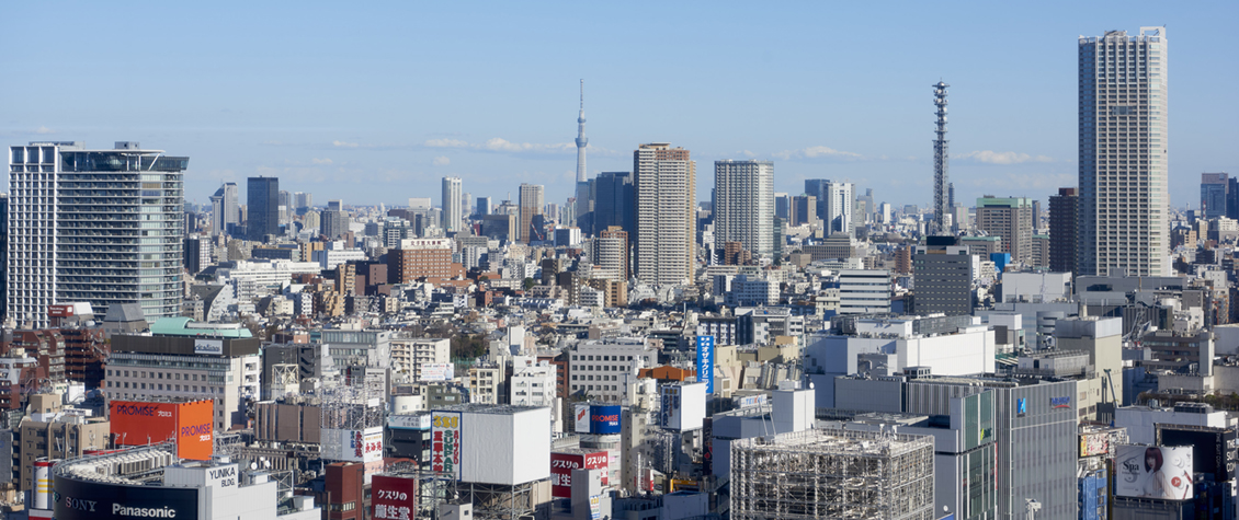
-
Shinjuku L Tower 22nd Floor, 1-6-1 Nishi-Shinjuku,
Shinjuku-Ku, Tokyo, 163-1522, JAPAN
TEL: +81-3-5322-6375
FAX: +81-3-4586-7302
- Our Team
-
Total Number of Employees 104 Attorneys 38 Japanese Patent Attorneys 29 ・Electrical Engineering, Electronics, Software 22 ・Chemical, Materials Science 5 ・Mechanics, Optics 16 ・Biotechnology 7 Trademark Attorneys 1 Design Attorneys 4 US Attorneys 6 ・Patent Attorneys 5 Chinese Patent Attorneys 1 ・Patent Attorneys 1 – Nearly all specialists are either attorneys or Ph.D.
– Numbers include overlaps, contracted employees and those of group companies
- Number of Applications Represented by RYUKA per year
-

The total number of domestic and foreign patent applications per year by domestic and foreign applicants.
International applications into or out of Japan are based on the nationalization date, pending applications transferred to our firm are based on the date of transferring, and all others are based on their actual filing date.
- Our Services
-
■Prosecution
Patents, Trademarks, Designs
■Technical Expertise
Information Technology, Software, Electrical Engineering, Electronics, Telecommunications, Mechanics, Optics, Biotechnology
■Legal Services
Patent Searches, Infringement or Non-Infringement Opinions, Negotiation, and Licensing
■Consultation Service
Full-service IP consultations from the invention harvesting, prosecution strategies to the post-grant IP managements
RYUKA Patent Translation Incorporated
The company provides high-quality translation of specifications for patent prosecutions. Our self-developed software, RYUKA Translation Assistant, assists the translators to consistently translate the applications, although it does not translate the applications by itself. The assisting software has significantly reduced translation fees and improved quality. Only specialized international IP law firms can provide such high-quality, cost-efficient translation.